ADC Oversampling - 2023
Oversampling is a class of methods to increase ADC resolution, signal-to-noise ratio (SNR), and/or the effective number of bits (ENOB) by taking multiple consecutive samples. I've encountered this process in my Flashlight project, where I used a voltage range of 0.1*VCC quantized by an 8-bit ADC for a feedback loop control. So let's take the same setup as a practical example and explore our options.
The circuit uses 8-bit ADC to measure voltage in a range from 0.9*VCC to VCC, so only about 25 (256*0.1) unique values can be measured and used for feedback control. That's too few for almost any feedback controller, so we will try to improve the resolution by averaging multiple samples. One sample takes 112us, so by averaging 64 samples we lower the sampling rate to 140Hz, which is still plentiful enough for a flashlight. For illustration purposes, we will test it on a triangular wave with an even tighter range of 0.96~VCC:
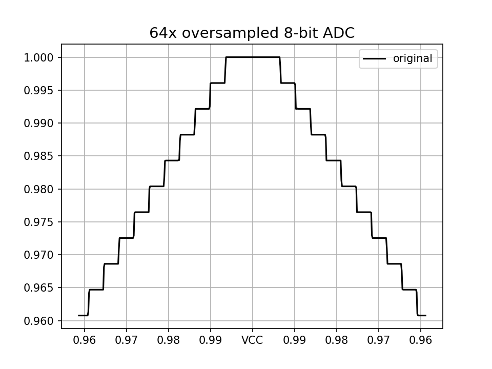
Well, what a bummer. Even though we achieved some rounding at the edges, we did not improve the resolution one bit. The problem lies in the noise and its amplitude. For the oversampling to be effective, the noise must be able to flip the lowest bit (LSB), so it needs to be at least 1 LSB in amplitude. Our input signal is very clean and does not satisfy this requirement.
In these cases, you can usually introduce some external noise by coupling a waveform generated by the microcontroller itself using either DAC or PWM. Such a system can also synchronize the waveform and ADC samples to achieve maximally repeatable results. In this case, however, we do not have an extra pin available, so we have to make the noise using the same GPIO pin we measure the signal.
One option our microcontroller offers is a pull-up resistor. So let's introduce a 2k2 input resistance in series with the input signal and turn on the pull-up resistor for exactly half of the measured samples. The pull-up, together with the input resistor, forms a voltage divider and should introduce a sufficient noise amplitude to increase the resolution:
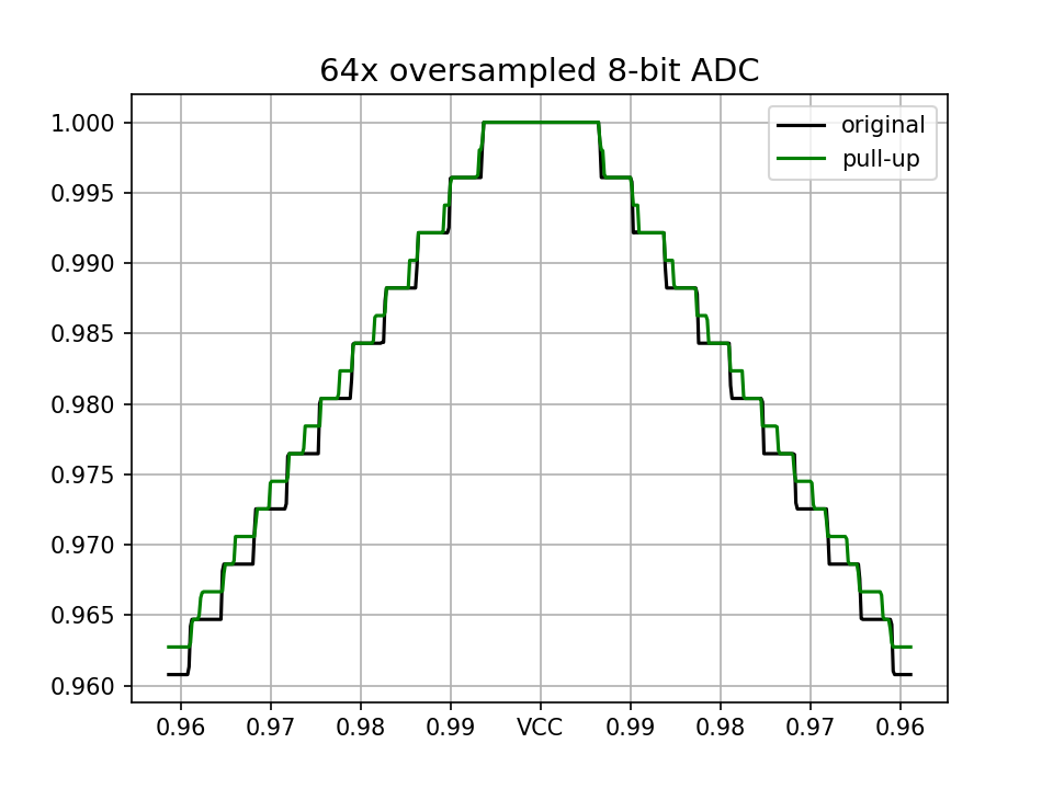
We do increase the resolution in some cases, but the problem is, that the pull-up introduces variable offset. Depending on the input voltage it either correctly flips the 1LSB, or just offsets the entire output value by 1bit, and these two cases periodically repeat over the whole ADC range. So... can we do better?
Let's add a capacitor and form an RC filter on the ADC input pin:
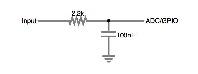
Before each measurement, the capacitor gets discharged by the GPIO pin, and afterward, 64 samples are taken as the capacitor is being charged by the input voltage. For the same voltage range as before, we get:
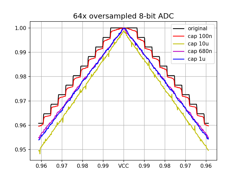
The 100nF capacitor does not change much, but capacitors 680nF, and 1uF achieve a significant increase in precision. The 10uF seems to experience some glitches, so to explore it further we look at the voltage on the ADC pin during measurement:
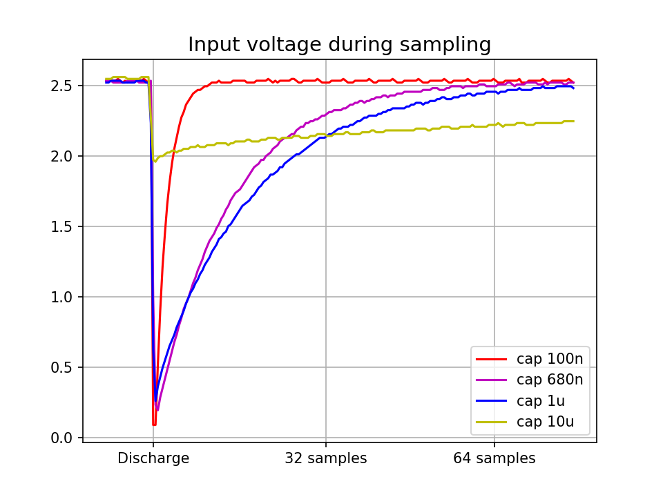
The capacitor is discharged for 100us, and 64 samples are taken immediately after for a total sample time of 7.3ms. The 100nF capacitor underperforms simply because it gets fully charged way too quickly. On the other extreme, the 10uF capacitor is not even able to get fully discharged, but more importantly, it has such a large time constant that it can not get to equilibrium before the next measurement starts. That explains the glitches visible in the previous plot and also shows the major weaknesses of larger capacitors, specifically, the low sample frequency limited by their charging time.
The 680nF and 1uF, on the other hand, offer both great sample time and better resolution.
It is also good to keep in mind that although great at small voltage ranges, the capacitor charging method introduces a nonlinearity over the full ADC input voltage range (from GND to VCC):
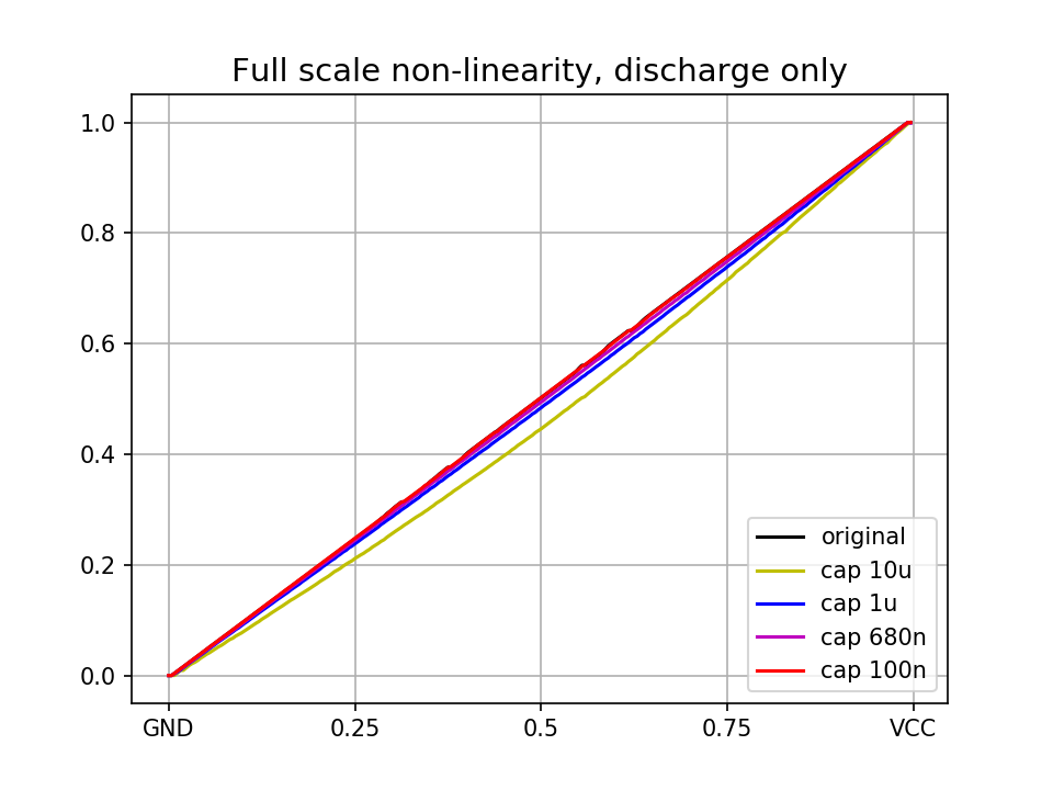
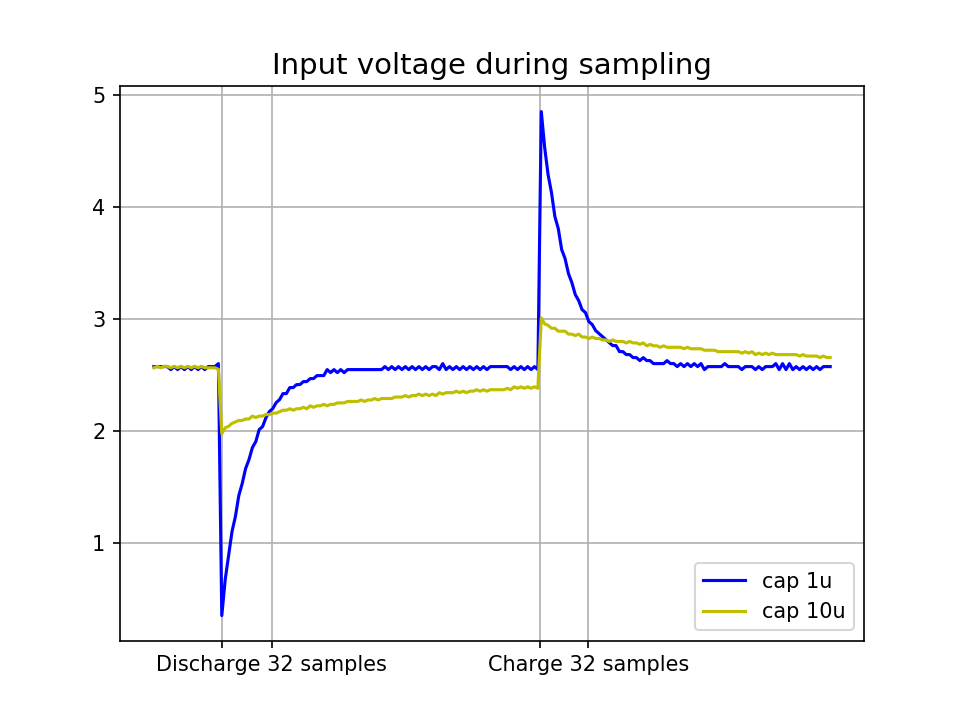
The nonlinearity gets bigger with larger capacitors, but it can be, at least marginally, reduced by performing two measurement cycles, one which discharges the capacitor as before and one that charges it. The voltage on the ADC input pin then looks like this:
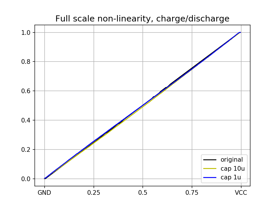
which results in a slightly better linearity:
Conclusion:
If there is a way to rescale the input signal to match the ADC voltage range, do that.
If there is a way to introduce sufficient noise levels for oversampling by using DAC or PWM with a low pass filter, do that.
If no option out of the ones above is possible, you may consider using an RC filter charging/discharging cycles and oversampling to increase your ADC performance.
I did not calculate the true ENOB achieved by this method, but it is better than 8-bits of the ADC, as evident in the 3rd plot. Keep in mind, that the feasibility of this method in any specific application and the nonlinearity it inevitably introduces is highly variable.
The code for Attiny10 used for acquiring the data in the plots above can be downloaded here.
Copyright © 2023 Jiri Stepanovsky. All Rights Reserved.