16-bit Serial Homebrew CPU - 2023
Building a homebrew CPU from scratch takes a large number of logic chips. It is understandable, that implementing registers, program counter, ALU, and other components of the CPU in TTL or CMOS logic does require a substantial amount of chips. But how many exactly?
I've tried to optimize my homebrew CPU for the lowest amount of logic chips possible and answer a question:
How few ICs are required for a Turing-complete CPU without a CPU?
My answer is a 16-bit Serial CPU with only 8 ICs, including memory and clock. It has 128kB SRAM, 768kB FLASH, and can be clocked up to 10MHz. It contains only a 1-bit ALU, but the majority of its 52 instructions operate on 16-bit values (serially). At its maximum speed, it executes roughly 12k instructions per second (0.012MIPS) and, among other things, is capable of streaming a video on PCD8544 based (Nokia 5110) LCD at ~10 FPS.
Depending on where you place the line between a state machine and a CPU, my 16-bit system might actually be the CPU with the lowest amount of ICs. Although, some other contestants are Jeff Laughton's 1-bit computer with 1 instruction and 1-bit of memory, and Daniel Thornburgh's Simple CPU with 1 byte-byte-jump instruction and memory simulated on a Raspberry PI.
Hardware:
The architecture is inspired by other CPU builds like James Sharman's JAM-1, Ben Eater's SAP-1, Warren's 4-bit Crazy Small CPU, its 8-bit version, and others. All of them, and many others alike, use a "control" EEPROM, EPROM, or ROM for generating control signals to the CPU components. Because it is way easier than generating them by logic circuits alone, and because it offers more flexibility in the future, I've also decided to use such a "control" memory, specifically, an EPROM. Contrary to the builds mentioned above, I've aimed for the lowest possible chip count, so I've tried to "squeeze" as much data processing inside the memory as possible, to either lower the demands on other CPU components or better yet, eliminate them completely. Here are some key steps taken:
- Completely eliminating the ALU and implementing it as a lookup. Because most EPROMs have only 8-bit output and the system also needs other control signals, the data width of the ALU has to be drastically limited. Not to worry, it can be reduced all the way down to a single bit: 1-bit computing is actually all we need.
- To get any meaningful computation done, the output from the 1-bit ALU has to be serialized. That is a perfect use case for a serial SRAM, which also brings other benefits. First, it eliminates the need for registers, since all ALU operations can be performed directly on the data in SRAM. Second, serial SRAMs are also addressed serially, so there is no need to latch the source and destination addresses. Third, an arbitrary data processing width can be achieved just by selecting the number of SRAM clock cycles. I chose 16 bits (16 SRAM clock cycles per 1 ALU operation) as a nice compromise between utility and speed.
- At least 2 serial SRAM chips are required, one of them has to provide a serialized input to our 1-bit ALU, and, at the same time, the second one has to store the result.
- For ALU operations with 2 operands (like ADD/AND/XOR...), 2 serialized inputs are needed. Adding a third SRAM could certainly be an option (2 for ALU inputs, 1 for result), but there is a better solution. If a serial FLASH memory is used instead of an SRAM, the same benefits remain (already serialized data, serialized address), but the FLASH can be used for storing the instructions/program as well as providing the ALU input.
- It is unnecessary to add any hardware for a program counter, as there is already plenty of space inside the SRAMs where its value can be stored.
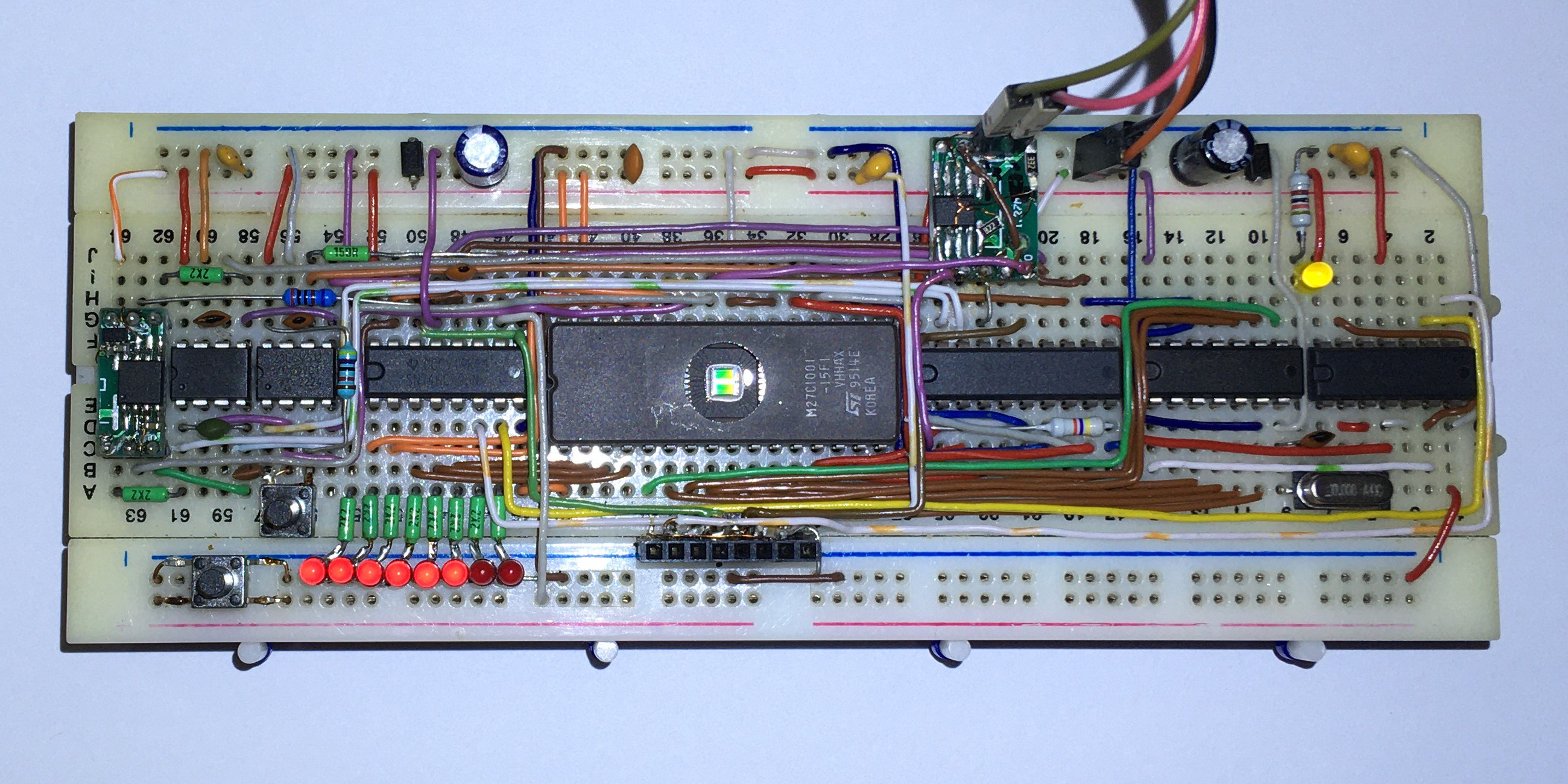
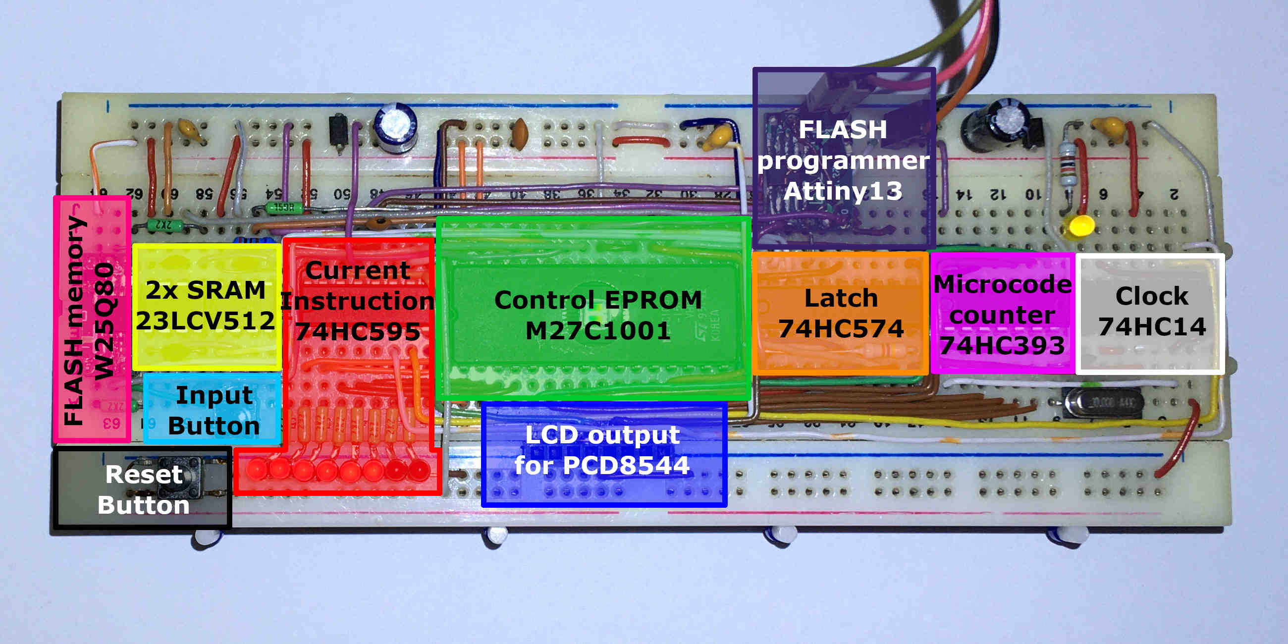
Even with these dramatic simplifications, some additional hardware is still required, however, everything can be built with just 8 chips in total, following the schematic below:

The circuit is built around a 128kB M27C1001-15 EPROM, working at 5V and combining a control state machine with a 1-bit ALU. Its output lines are latched by a 74HC574 every clock cycle and control the two 23LCV512 64kB serial SRAMs and one W25Q80 1MB serial FLASH. There are not enough outputs to control each memory individually, so they share the data line and partially also the chip select line, only the clock lines are kept separate. I could not find a 5V serial FLASH memory, so resistors R3, R4, and R5 limit the current and form a bridge from 5V to 3.3V. I do not count the MCP1703 3.3V voltage regulator as part of the CPU (I consider it, to be a part of a power supply), but with it, my CPU contains 9 chips.
The current instruction is stored in a buffered shift register 74HC595, which has its control lines also partially shared with the memories. Every instruction takes a couple of cycles to complete, so the progress within an instruction is tracked by a "microcode" counter 74HC393. After the instruction completes, the "Counter_reset" line resets the "microcode" counter and starts the execution of the next instruction buffered in 74HC595.
The 74HC574 and the "microcode" counter 74HC393 use opposite clock edge, so the clock generator 74HC14 provides an inverted clock signal to the 74HC393 to make them both synchronous.
Inputs and Outputs:
One thing I was not able to reasonably implement in my CPU is a self-programming of the FLASH memory. Bootloader is, therefore, not possible, and uploading a new program to the serial FLASH must be done externally. For this purpose, I used an Attiny13 microcontroller that listens to a set of commands over a UART, so any USB-UART adapter is sufficient for uploading a new code. When programming, it disables the output of the 74HC574 via the "Prog_en" line and proceeds to program the FLASH memory directly. The microcontroller is used only for uploading a new program and the CPU is happily running without it.
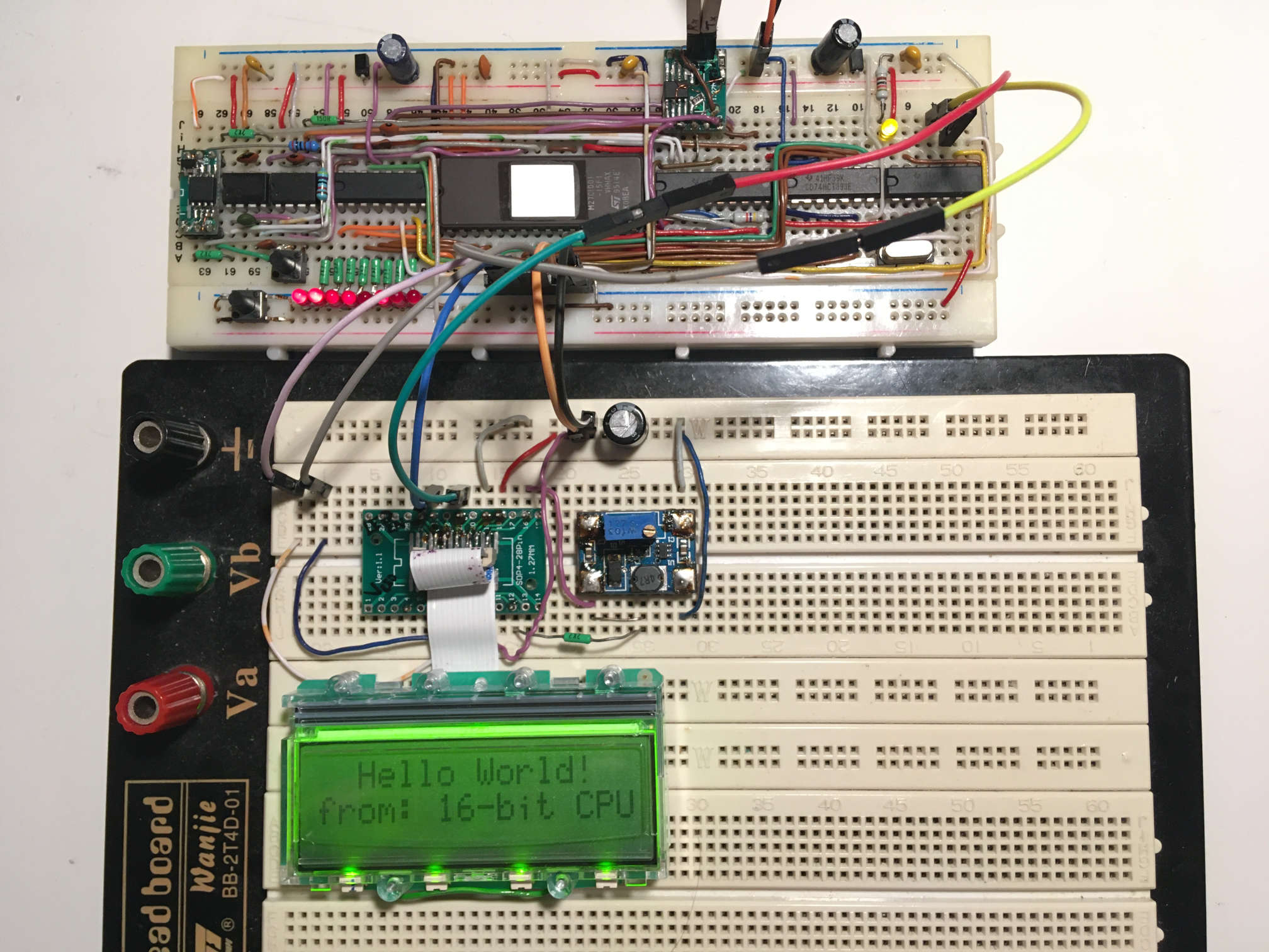
The only available outputs are the two upper bits of the instruction shift register 74HC595. I used one of these inverted lines as a chip select, which allows the CPU to connect to an SPI-like device. For example, a 3.3V PCD8544-based SPI LCD (Nokia 5110) can be connected directly, with the second upper instruction bit acting as the LCD data/command selector.
Another option is connecting an additional 74HC595 shift register instead of an LCD to get classic digital output lines.
The only available inputs are the two memory data/input signals connected to the EPROM address lines (A9, A11). The serial memories keep these signals at high impedance when they are not in use, so they can be sampled as general digital inputs when the memories are idle. It is important to note that the input signal must not interfere with the memory data, so a high resistance between the input signal and the memory input line is required (R6, R7). Sidenote: reading the input signal on memory data lines is working for clock frequencies only up to about 8MHz. At higher frequencies, the sampled data seem to be erratic and the CPU is prone to stalling.

You could already see my CPU playing the "Bad Apple!!" music video on a PCD8544 LCD somewhere on top of this page. In the video below, I demonstrate the possibility to control general digital outputs by adding another 74HC595. The same circuit can be used to produce 8-bit music at up to 4300 samples per second if an R-2R ladder is used instead of LEDs, and it is the same circuit I used to produce the soundtrack for the "Bad Apple!!" video.
Memory map:
The CPU has no dedicated registers, but it has two SRAMs that it can read from and write to. The downside is that each time the CPU wants to access data, it has to write the full 16-bit address to the serial SRAM. The upside is that because it has to write the full 16-bit address anyway, the CPU (and instructions in general) can access all of the 64kB of the SRAM at a constant time.
I've selected one SRAM (U8/RAM1) to be used for holding the program data, and all arithmetic and logical operations are designed to be performed on values within this memory. The second SRAM (U7/RAM2) is meant to be used for a stack, so only a few instructions are able to access and modify its contents.
The first few bytes of both memories are reserved for storing the internal CPU state like the program counter, the flag bit, the stack pointer, an intermediate result, the source/destination addresses, and other internally used values. The approximate memory map is in the table below:
| Address: | 0x0 | 0x1 | 0x2 | 0x3 | 0x4 | 0x5 | 0x6 | 0x7 | 0x8 | 0x9 | 0xA | 0xB | 0xC | 0xD | 0x000E~0xFFFF |
| RAM1: | Flag & Input | Program counter (PC) | Program counter reversed | Stack pointer (SP) | Stack value (SPVAL) | Registers and user data | |||||||||
| RAM2: | Flag | Program counter (PC) | Destination address | Instruction's result | Stack and user data | ||||||||||
One thing I would like to mention is the method of using the FLASH memory as the second ALU input. Because the FLASH is quite large (1MB), it is possible to fit inside it a full 16-bit lookup table containing 16-bit identical values. With this 128kB lookup, it is then possible to write a 16-bit value to the FLASH as an address and read back the same 16-bit value as data, which can be used as an ALU input.
A slight inconvenience of using the serial memories is that they are addressed in an MSB-first format, while the 1-bit ALU naturally computes in an LSB-first format. To get a functional memory addressing, we need to reverse the bits from the LSB-first format the CPU works with to the MSB-first format the memories work with. Reversing bits using a 1-bit ALU is not straightforward, so I've reserved another 128kB of FLASH memory for a "reversed-values" lookup table to make the operation faster. It works the same way as the previous lookup, a value is written to the FLASH memory as an address and its reversed representation is read back as data.
These two 16-bit lookup tables are the reason my CPU has only 768kB of FLASH memory and why the program counter (PC) starts at address 0x040000 and not zero.
Instruction set:
There are some restrictions for the instruction set arising from the limited hardware. The CPU is capable of only 64 unique instructions/operations, all of which have to fit in the maximum of 256 micro-instruction steps and must get by working with only a 1-bit ALU and 1 Flag bit. But even with these limitations, surprisingly, it is possible to create quite a nice-looking instruction set:
| OP code | Name | Operands | Width | Flag | Cycles | Total | Description |
| 0x00 | INIT | - | - | clear | 256 | 256 | Wait for clock to stabilize, then initialize RAM ICs to sequential mode |
| 0x01 | RESET | - | - | clear | 235 | 235 | Set program counter PC = 0x040000 and stack pointer SP = 0x000A |
| 0x02 | - | - | - | - | 158 | 414 | Shadow instruction: Fetch |
| 0x03 | - | - | - | - | 256 | 414 | Shadow instruction: Fetch continuation |
| 0x04 | - | - | - | - | 129 | 129 | Shadow instruction: Increment program counter PC = PC + 3 |
| 0x05 | - | - | - | - | 129 | 129 | Shadow instruction: Increment program counter PC = PC + 5 |
| 0x06 | - | - | - | - | 129 | 129 | Shadow instruction: Increment program counter PC = PC + 7 |
| 0x07 | - | - | - | - | 129 | 129 | Shadow instruction: Increment program counter PC = PC + 8 |
| 0x08 | - | - | - | - | 162 | 291 | Shadow instruction: Copy 32 bit result |
| 0x09 | - | - | - | - | 130 | 259 | Shadow instruction: Copy 16 bit result |
| 0x0A | - | - | - | - | 113 | 113 | Shadow instruction: Copy program counter |
| 0x0B | - | - | - | - | 167 | 296 | Shadow instruction: Store to RAM indirect |
| 0x0C | - | - | - | - | 151 | 280 | Shadow instruction: Store to RAM indirect |
| 0x0D | - | - | - | - | 173 | 587 | Shadow instruction: Arithmetic instruction dispatch |
| 0x0E | STF | - | - | set | 132 | 546 | Set FLAG |
| 0x0F | CLF | - | - | clear | 132 | 546 | Clear FLAG |
| 0x10 | NOP | - | - | - | 132 | 546 | No operation |
| 0x11 | MOV | addr16 <- addr16 | 16 | - | 231 | 774 | Move 16 bit value |
| 0x12 | MOVW | addr16 <- addr16 | 32 | - | 146 | 851 | Move 32 bit value |
| 0x13 | INC | addr16 <- addr16 | 16 | overflow | 231 | 774 | Increment |
| 0x14 | DEC | addr16 <- addr16 | 16 | overflow | 231 | 774 | Decrement |
| 0x15 | COM | addr16 <- addr16 | 16 | zero | 231 | 774 | 1's complement (NOT) |
| 0x16 | NEG | addr16 <- addr16 | 16 | zero | 231 | 774 | 2's complement |
| 0x17 | LSL | addr16 <- addr16 | 16 | overflow | 233 | 776 | Left shift (<<) |
| 0x18 | LSR | addr16 <- addr16 | 16 | overflow | 233 | 776 | Right shift (>>) |
| 0x19 | ROL | addr16 <- addr16 | 16 | overflow | 233 | 776 | Left shift with carry |
| 0x1A | ROR | addr16 <- addr16 | 16 | overflow | 255 | 798 | Right shift with carry |
| 0x1B | ASR | addr16 <- addr16 | 16 | overflow | 235 | 778 | Arithmetic right shift (keeps sign bit) |
| 0x1C | REV | addr16 <- addr16 | 16 | - | 238 | 781 | Bit reverse |
| 0x1D | ADDI | addr16 <- addr16, val16 | 16 | overflow | 231 | 774 | Add immediate |
| 0x1E | ADCI | addr16 <- addr16, val16 | 16 | overflow | 231 | 774 | Add immediate with carry |
| 0x1F | SUBI | addr16 <- addr16, val16 | 16 | overflow | 231 | 774 | Subtract immediate |
| 0x20 | SBCI | addr16 <- addr16, val16 | 16 | overflow | 231 | 774 | Subtract immediate with carry |
| 0x21 | ANDI | addr16 <- addr16, val16 | 16 | zero | 231 | 774 | Logical AND with immediate |
| 0x22 | ORI | addr16 <- addr16, val16 | 16 | zero | 231 | 774 | Logical OR with immediate |
| 0x23 | XORI | addr16 <- addr16, val16 | 16 | zero | 231 | 774 | Logical XOR with immediate |
| 0x24 | ADD | addr16 <- addr16, addr16 | 16 | overflow | 171 | 887 | Add register |
| 0x25 | ADC | addr16 <- addr16, addr16 | 16 | overflow | 171 | 887 | Add register with carry |
| 0x26 | SUB | addr16 <- addr16, addr16 | 16 | overflow | 171 | 887 | Subtract register |
| 0x27 | SBC | addr16 <- addr16, addr16 | 16 | overflow | 171 | 887 | Subtract register with carry |
| 0x28 | AND | addr16 <- addr16, addr16 | 16 | zero | 171 | 887 | Logical AND with register |
| 0x29 | OR | addr16 <- addr16, addr16 | 16 | zero | 171 | 887 | Logical OR with register |
| 0x2A | XOR | addr16 <- addr16, addr16 | 16 | zero | 171 | 887 | Logical XOR with register |
| 0x2B | JMP | addr24 | - | - | 197 | 611 | Jump to address |
| 0x2C | CALL | addr24 | 32 | - | 221 | 748 | Copy following instruction's address (PC + 4) and current FLAG to SPVAL, then jump |
| 0x2D | RET | - | 32 | restore | 138 | 552 | Move SPVAL to PC & FLAG (effectively returns from CALL and restores previous FLAG) |
| 0x2E | BRFS | addr24 | - | - | 160 | 625|574 | Branch if FLAG set |
| 0x2F | BRFC | addr24 | - | - | 160 | 625|574 | Branch if FLAG cleared |
| 0x30 | BREQ | addr16, addr24 | 16 | - | 243 | 708|657 | Branch if register is zero |
| 0x31 | BRNE | addr16, addr24 | 16 | - | 243 | 708|657 | Branch if register is not zero |
| 0x32 | LDI | addr16 <- value16 | 16 | - | 81 | 624 | Load 16 bit immediate |
| 0x33 | LDIW | addr16 <- value32 | 32 | - | 113 | 656 | Load 32 bit immediate |
| 0x34 | LD | addr16 <- [addr16] | 16 | - | 238 | 911 | Indirect load 16 bits from address |
| 0x35 | LDB | addr16 <- [addr16] | 8 | - | 238 | 911 | Indirect load 8 bits from address, set upper 8 bits to 0 |
| 0x36 | ST | [addr16] <- addr16 | 16 | - | 163 | 873 | Indirect store 16 bits to address |
| 0x37 | STB | [addr16] <- addr16 | 8 | - | 163 | 857 | Indirect store 8 bits to address |
| 0x38 | LD2W | [addr16] | 32 | - | 256 | 799 | Indirect load 32 bits from address in RAM2 to SPVAL register |
| 0x39 | LD2 | [addr16] | 16 | - | 224 | 767 | Indirect load 16 bits from address in RAM2 to SPVAL register |
| 0x3A | ST2W | [addr16] | 32 | - | 256 | 799 | Indirect store 32 bits from SPVAL register to address in RAM2 |
| 0x3B | ST2 | [addr16] | 16 | - | 224 | 767 | Indirect store 16 bits from SPVAL register to address in RAM2 |
| 0x3C | LPM | addr16 <- [addr16] | 16 | - | 211 | 884 | Indirect load 16 bits from address in FLASH |
| 0x3D | LPB | addr16 <- [addr16] | 8 | - | 211 | 884 | Indirect load 8 bits from address in FLASH, set upper 8 bits to 0 |
| 0x3E | OUT | addr16 | 8 | - | 252 | 795 | Output 8 bits over SPI |
| 0x3F | HALT | - | - | clear | 14 | 428 | Stop execution |
The first instructions, INIT and RESET, are executed at power-up or when the RESET button is pressed. The "shadow" instructions are non-user-accessible instructions, primarily used for repeating operations like fetching an instruction, program counter increment, result write-back, and similar.
Arithmetic and logical operations use the one Flag bit as either a Carry/Overflow or a Zero flag. As mentioned above, there is no performance penalty for accessing the full address space, so all these instructions can specify any source/destination address within the 64kB SRAM address space. Indirect addressing for arithmetic operations is not supported directly but must be performed by LD/ST (load/store) instructions.
The second set of LD2/ST2 instructions is accessing the second SRAM. They are meant to be used for stack, but any data can be stored. PUSH and POP instructions are not implemented, but they can be constructed from LD2/ST2 and INC/DEC instructions.
An average instruction takes about 800 clock cycles, including fetch operation and program counter increment. At the maximum clock frequency of 10MHz, the CPU can execute about 12k instructions per second.
Writing code in assembler:
I use Lorenzi's customasm tool to generate binary files from assembly source code. The binary files can then be uploaded using a small python3 application to the Attiny13 programming microcontroller that writes the binary into the FLASH.
Below are two examples of small subroutines written in assembler for my CPU. The first subroutine returns the 32-bit result of two 16-bit values multiplication. The second one writes an ascii string stored inside the FLASH memory to the LCD.
| Multiply32_16x16 | LCD_WriteStrF |
; Returns FA32 = FA16 * FB16
; FB is expected to be smaller
Multiply32_16x16:
    ;PUSH_PC        ; Not necessary
    LDIW FC, 0      ; Clear result
    LDI FA+2, 0     ; Cast FA16 to FA32
.loop:
    ANDI TMP, FB, 1
    BRFS .skip_add
    ADD FC, FA      ; Add FC32 += FA32
    ADC FC+2, FA+2  ; Add FC32 += FA32
.skip_add:
    LSL FA          ; Shift FA32 << 1
    ROL FA+2        ; Shift FA32 << 1
    LSR FB          ; Shift FB16 >> 1
    BRNE FB, .loop
    MOVW FA, FC     ; Copy result
    ;POP_PC         ; Not necessary
    RET
|
; Write String in Flash
; input: FA32 <- Address of the string in Flash
LCD_WriteStrF:
    PUSH_PC             ; Save return address
    PUSHW RA            ; Save RA 32-bit
    MOVW RA, FA
.loop:
    LPB FA, RA          ; Load character from Flash
    BREQ FA, .stop      ; Test "\0" character
    REV FA              ; MSB-first -> LSB-first
    ANDI FA, FA+1, 0xFF ; Cast to 8bits
    CALL LCD_WriteChar  ; Write character
    ADDI RA, 1          ; Increase 32-bit pointer
    ADCI RA+2, 0        ; Increase 32-bit pointer
    JMP .loop
.stop:
    POPW RA             ; Restore RA 32-bit
    POP_PC              ; Restore return address
    RET
|
Maximum Frequency and the Critical path:
According to specifications, the total propagation delay across the critical path is:
- 12ns at 74HC14 from "Clock_pos" to "Clock_neg",
- 54ns at 74HC393 to ripple to the last 8th bit (12+3x5+12+3x5 ns),
- 150ns access time at M27C1001-15 EPROM,
- 2ns at 74HC574 to stabilize the inputs before the clock edge.
Putting it together, the circuit should only be able to run at ~4.6MHz. My specific build, however, is able to work flawlessly up to 10MHz and becomes unstable only above ~10.5MHz. For a circuit built on a breadboard with plenty of parasitic capacitance, I consider it quite impressive. The maximum clock rate might even be improved if a faster binary counter or faster EPROM were used.
Conclusion and Retrospective:
I am really pleased with the finished CPU. It has nice and "easy-to-work-with" instruction set with all the basic instructions present. It is powerful enough to stream a video on a small LCD screen, play audio (though using an external "sound card"), and generally perform the simple input/output computational operations it was originally intended for. Finally, it successfuly demonstrates that it is possible to build a functional homebrew CPU with only a handful of ICs.
There are, however, some small improvements possible:
- The 74HC393 ripple counter is a significant bottleneck in the critical path. Replacing it with a carry-lookahead adder ("fast adder") or with a buffered counter like 74HC590 would increase the maximum clock speed.
- The same goes for the M27C1001-15 EPROM. Using a faster memory like M27C1001-35 EPROM or SST39SF020A-70 FLASH would also allow higher clock rate.
- A larger EPROM with more than 17 address lines could be used to either increase the instruction count or to utilize the additional address lines as general digital inputs.
- Adding some instructions for erasing and programming the internal FLASH memory would have enabled a bootloader to be made, which would make the Attiny13 programming circuit unnecessary.
- The system is able to execute code only from the FLASH memory. It would be possible to create an emulator inside the FLASH and make the emulator execute code from SRAM but to make the CPU execute code from SRAM natively, a different instruction fetching process would be required, possibly including a duplicate set of instructions just for the SRAM execution itself.
I will have yet to see if some of these improvements seem to be worthwhile to implement. In the meantime, if you like the project and want to dive deeper, you can skim through the source code available here. It contains a simulator, EPROM microcode generator, Attiny13 programmer firmware, and all of my assembler codes.
Update:
I've implemented a minimalistic 3D wireframe object projection engine using 16-bit fixed-point arithmetic. Multiplying matrices on my 0.012 MIPS CPU is quite slow, so 3D games are probably not coming anytime soon:
I'm also slowly growing the list of hardware my CPU directly supports. I've added an SPI alphanumeric LCD I've salvaged from an old HP printer:
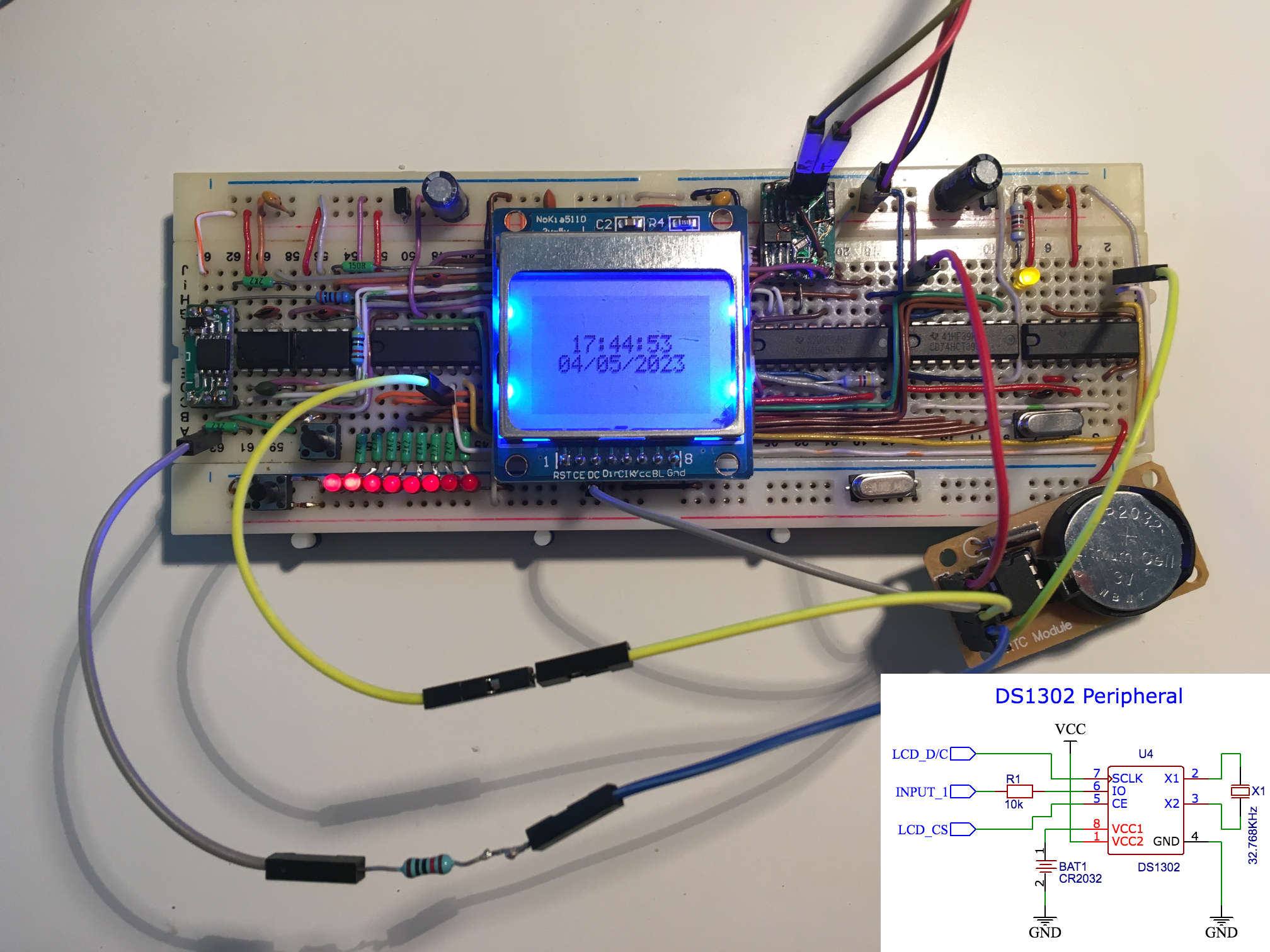
and I've been able to "bit-bang" the serial interface for DS1302 real-time clock. The software does have to use some special instruction sequences to produce the necessary signals, but it is possible and does not require any additional hardware.
Update 2:
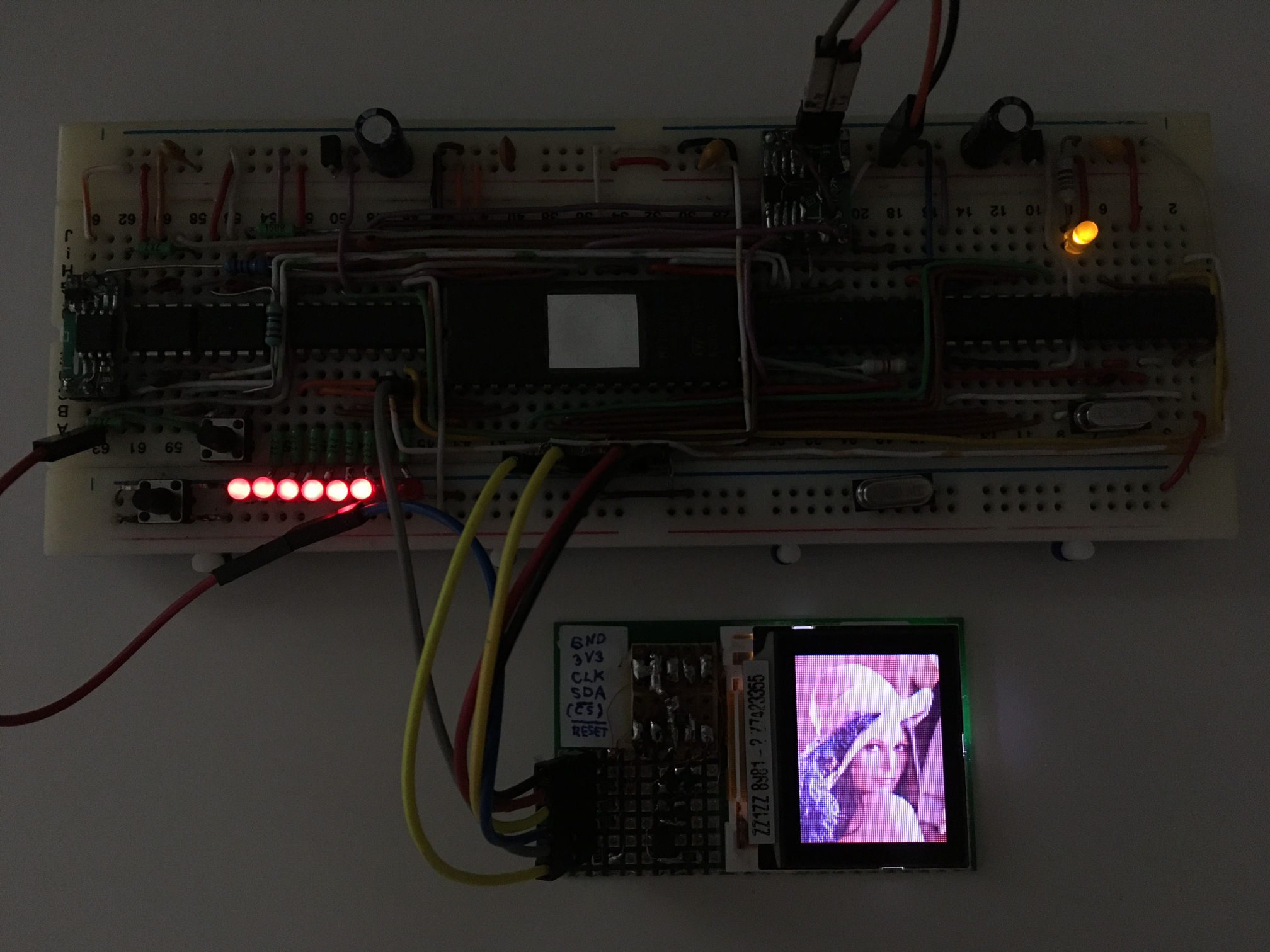
The CPU now supports a PCF8833 LCD driver, although one frame takes about 96 seconds to render.
Homebuilt CPUs WebRing
Definitely check out other awesome homebrew CPU builds on Warren's https://www.homebrewcpuring.org
Join the ring?
To join the Homebuilt CPUs ring, drop Warren a line (mail is obfuscated, you have to change [at] to @), mentioning your page's URL. He'll then add it to the list.
You will need to copy this code fragment into your page (or reference it.)
Note: The ring is chartered for projects that include a home-built CPU. It can emulate a commercial part, that′s OK.
But actually using that commercial CPU doesn′t rate. Likewise, the project must have been at least partially built: pure paper designs don′t rate either.
It can be built using any technology you like, from relays to FPGAs.
Copyright © 2023 Jiri Stepanovsky. All Rights Reserved.